DC Gain Analysis
When implementing the Thomas Henry design [ref], I found that there was a persistent DC offset (\pm 100-300\mathrm{mV}) at the filter outputs. Ray Wilson made a comment noting this behaviour in the MFOS version and resolved it by adding DC blocking capacitors before buffering the output.
However, when testing I found that the DC offset at the LP filter output was strongly dependent on the resonance setting and was as large as 1.5V with minimum resonance. While the HP and BP outputs had consistent signs (each stage is non-inverting), the LP output had an additional unexpected sign flip.
The following is an attempt at a more in-depth analysis of the gain in the feedback loops. I'm starting with a few constraints/assumptions:
- The input voltage is 0V
- The resonance pot is at its minimum but should be kept in the analysis to understand its impact (R_r for the resonance feedback loop is R3=22k at minimum resonance)
- The amplifier bias currents into the OTAs are nominal and matched.
- Ignore the notch filter (summing amplifier)
While checking this in a simulation, I noticed that the design is mainly sensitive to offsets in the OTA inputs. Therefore, I'll also assume ideal opamps (v_n = v_p).
Note: the subscripts generally refer to the symbol identifiers in the schematic, e.g. the inverting input of U1A has voltage v_{n1a}.
First Stage: Inverting Summing Opamp
In a simplified analysis (A_1 \to \infty), v_{n1a} = v_{p1a}= 0 = \Delta v_{1a}.
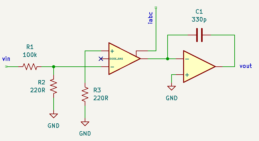
Second Stage: Filter
Stage two combines an OTA and U1B. The inverting input of the OTA is fed by a resistor divider with a gain of A_{r} = 0.0022. The gain through the OTA is
i_{o2a} = -19.2 i_{abc}\left(v_{n2a}-v_{p2a}\right)
The DC offset behaviour should be independent of the amplifier bias current i_{abc}. This appears to be true in practice: measuring the offsets shows a very weak dependence on the bias current set by the cutoff control. Setting i_{abc}=52\mu A results in a gain factor of A_{gm} = 1\mathrm{mA/V}, or
i_{o2a} = -A_{gm}\left(v_{n2a}-v_{p2a}\right)
The non-inverting input of the OTA is grounded, but allowing for an offset (typical up to 0.4mV per datasheet),
i_{o2a} = -A_{gm}\left(A_{r} v_{o1a} - \Delta v\right)
This current is fed through to the integrator. The filter stage in the Thomas Henry design puts the integrating capacitor in the feedback path of the opamp,
The linearized AC gain through this block can be found starting with KCL into v_{n1} (the inverting input of the opamp). Assuming an ideal opamp, v_{n1} = v_{p1} = 0,
where \Delta v_1 is the offest in the first OTA.
Substituting for v_{o1a}
Third Stage: Filter
The topology of the third stage matches the second, with the input from stage 2: v_{i} = v_{o1b}. The transfer function with OTA offset \Delta v is
Substituting for v_{o1b}
DC Response
Letting sC \to 0 in the previous expression yields the DC dependence of the LP output on the OTA offset voltages:
Since A_r \ll 1, the attenuating resistive divider contributes significantly. Also, the dependence on the resonance feedback resistor is seen in A_x = \frac{100\mathrm{k}}{R_r}: \Delta v_2 can contriubte 5x more than \Delta v_1.
To get a DC expression for v_{o1b} (BP output), let sC \to 0 in the previous expression for v_{o1b} and substitute v_{o1c}:
This is independent of the resonance feedback. Using the typical datasheet offset value 0.3mV, this contributes a DC value of -136mV.
Finally, the DC expression for v_{o1a} (HP output) is
This behaviour can be verified in a Falstad simulation.
Observations
The DC offsets are only a function of four parameters: the offsets of the two OTAs, the gain of the resistor divider, and the weighting of the resonance feedback in the summing amplifier. Consequently, the offests are
- Independent of the type of OTA (offset voltage dependent)
- Independent of the amplifier bias current (confirmed via measurments and simulations)
- Dominate over offsets from the opamps (confirmed via measurements and simulations)
In addition
- the non-intuitive sign behaviour comes out of the derivation (the DC offset at the LP filter has the opposite sign as the HP & BP outputs)
- the DC offset at the BP output (v_{o1b}) only depends on the input offset in the last stage (\Delta v_2); it's independent of the resonance feedback
- similarly, the DC offset at the HP output (v_{o1a}) only depends on the input offset in the middle stage (\Delta v_1); it's independent of the resonance feedback
- the DC offset for the LP output depends on the resonance feedback
The last few points are important: trimming out the offset will only work if both \Delta v_1 and \Delta v_2 are reduced to zero, and that must be checked independently at the HP and BP outputs.
References
- Thomas Henry, "VCF-1", birthofasynth.com
- Ray Wilson, "State Variable VCF 12dB/oct with VC Resonance", MFOS
- "LM13700 Dual Operational Transconductance Amps w/Linearizing Diodes and Buffers datasheet", Texas Instruments