Analog Gate Delay Theory
References
- Aaron Lanterman, "ECE4450 L18: Exponential Voltage-to-Current Conversion & Tempco Resistors", [youtube]
- Hal Chamberlain, Musical Applications of Microprocessors, 2nd Ed., Hayden Books, 1985
- Paul Horowitz and Winfield Hill, The Art of Electronics, 3rd Ed., Cambridge University Press, 2015
- Rene Schmitz, "A tutorial on exponential converters and temperature compensation", [schmitzbits.de]
- Paul Gray, et al., Analysis and Design of Analog Integrated Circuits, 4th Ed., Wiley, 2001
Delay Timing
The delay timing is set the IV relationship for the capacitors:
where t_d is the delay time, C is the capacitance of the timing capacitors, and V_P is the positive threshold voltage of the Schmitt trigger inverter.
Constraints
- V_P = 6V
- C = 100nF
- let the current range from 0.5uA to 500uA
- nominal control voltages range from 0 to 5V
With these assumptions,
Exponential Voltage to Current Conversion
This sub-circuit design is presented in the Building Blocks section: Linear to Exponential Voltage Conversion. Relevant adjustments to that core design are detailed below.
For the analog delay, an inverting relation between the linear input voltage and the exponential current is required: increasing the control voltage should increase the delay time, which implies reducing the current supplied to the integrating capacitors. Therefore, the base of the BJT in the reference current feedback loop is grounded, such that
To establish the desired gain of an input stage, let v_{b2} = A v_{in}. When the input voltage travels over the full range (0-5V), the programming current should decrease by a factor of 1000 (500uA to 0.5uA):
The value of I_{ref} will be equal to i_{p,max} when v_{in} = 0. This will set the shortest delay time.
Using an op-amp in an inverting gain and a voltage divider to supply v_{b2}
where R'_2 is adjusted such that the voltage divider gives a gain of \frac{27}{28}.
Temperature compensation is independent of the input gain, so the same analysis given in the Building Block applies, including the approaches to approximate a 3400ppm/C PTC thermistor. The updated schematic is shown below.
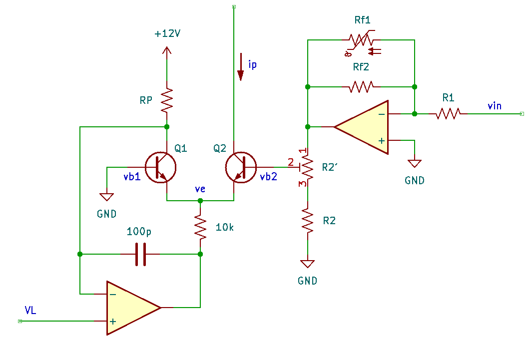
With R_{f1}\parallel R_{f2} = 5.454\mathrm{k}\Omega (10k PTC thermistor in parallel with a 12k resistor), R_1 = 150\mathrm{k}\Omega gives an approximate gain in the inverting amplifier of 0.03633 (1/27.5) per the design requirement (the remaining fraction can be tuned in a 100\Omega trim pot in series with a 2.2\mathrm{k}\Omega resistor in the voltage divider).
Current Mirror
This derivation follows section A.4.1.1 (appendix 1.1 in chapter 4) of Gray's book (ref. 5).
The programming current is mirrored to both the capacitors (corresponding to the leading edge and trailing edge delay timing). The key design requirement is the match between these two copies of the current: errors in the ratio of the copy to the programming current are more tolerable.
The base voltages (relative to ground) of all transistors in the current mirror are equivalent by construction:
Taking the difference of these equations for Q2 and Q3 (note: in Gray, there is a beta helper as Q2, so the numbering is different)
Defining average and mismatch parameters, e.g. i_c = 1/2(i_{c2}+i_{c3}) and \Delta i_c = i_{c3}-i_{c2}, and using assumptions
- Delta i_c / 2i_c \ll 1
- \ln (1+x) \simeq x if x \ll 1
the voltage equation yields the following relationship for the current error (see Gray Eq. 4.296):
Recall that \alpha_F = \frac{\beta_F}{1 + \beta_F} \approx 1 and g_m = i_c/V_T such that the term A is the ratio of the (average) voltage drop across R_E to V_T. This leads to the following conclusions
- If A \gg 1, the effect of the mismatch between transistors Q2 and Q3 is reduced by \sim 1/A.
- The negative sign in the second term indicates that an intentional difference between R_{E2} and R_{E3} can be used to cancel the error due to \alpha_F.
- R_E increases the output impedance of the transistor, reducing the current error due to the dependence of i_c on v_{ce} (Early effect). This can reduce the error \epsilon \propto \Delta i_c / i_c from \epsilon ~ \frac{\Delta v_{ce}}{V_A} to \frac{\Delta v_{ce}}{V_A(1+A)}.
Combined, emitter degeneration with a voltage drop of >10V_T and an intentional difference can significantly reduce the current mismatch in the output branches of the current mirror. However, this is limited by the requirement to maintain the transistors in the forward active region: V_{cc} - V_{out,max} = v_{ce,sat.} + i_{e}R_E. Given
- V_{cc} = 11.4 V
- V_{out,max} = 9.1 V (Zener voltage)
- v_{ce,sat.} = 0.3 V (BC557)
- i_{c,max} = 500\mu A (design)
then R_E < 5.2\mathrm{k}\Omega (choose R_E =4.7\mathrm{k}\Omega). Note that V_{RE} ~ 0 when the current drops below 10\mu\mathrm{A}, so this approach has limited effectiveness for low currents (longer delay times).