VCA Design
Calcultions can be found in the notebook.
Linear V-to-I Converter
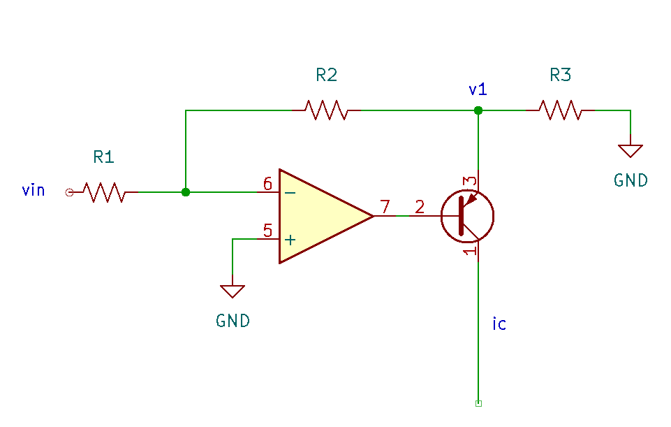
Following the derivation for the linear V-to-I converter, the output current I_{out} is found assuming
- an ideal op-amp (v_n = v_p = 0)
- negligible base current (i_e = i_c + i_b \approx i_c)
such that
The input CV is assumed to be a positive envelope with a range from 0 to 10V. The control current for the OTA should not exceed 1mA. The input impedance is R_1 = 100k\Omega. With these constraints,
Note
v_1 = -\frac{R_2}{R_1}v_{in} and that the output of the opamp connected to the base of the PNP will be limited to around \pm 10.5V. To ensure that the opamp can still control the PNP, v_1 \gtrsim -10.5V when v_{in} \to +12V: choose R_2 < R_1.
Choosing R_3 = 15k\Omega and R_2 = 68k\Omega ensures that nominally the current is limited to less than 500uA (max.: 700uA). A diode in the feedback loop ensures that negative voltages are not passed to the BJT. The gain of the CV stage is then
and at an input level of 8V, the output current is 442.7uA.
OTA and Output Buffer
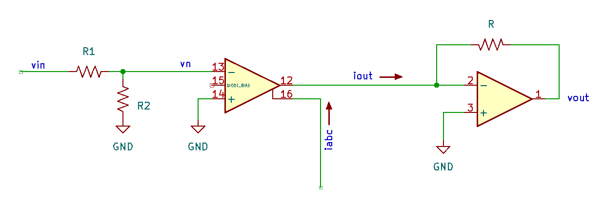
For the OTA, the transconductance is
where i_{abc} is the amplifier bias current and the thermal voltage V_T = 25.6 mV at room temperature. The output current is given by
The amplifier bias current should fall in the range of 1uA to 1mA.
For this analysis, assume that v_p = 0 (the non-inverting input can be trimmed to remove any DC offset). Consequently, the output current is i_{out} = -19.2 i_{abc} v_n, which then passes through the resistor R in the feedback loop of the op-amp to produce a voltage output of (two inverting stages cancel the sign)
A voltage divider is used to reduce the input signal voltage: v_n = \frac{R_2}{R_1 + R_2} v_{in} with R_2 \ll R_1. The linear region for the OTA is nominally in the range where |v_{p} - v_{n}| < 10mV. Assuming a 10Vpp input signal, choose the ratio for R_2 and R_1
For R_1 = 100k\Omega, R_2 = 220\Omega will approximately satisfy this condition. The gain of the OTA stage is then
This design will assume unity gain for the audio signal with a 8V CV input (matching the peak voltage from a 555-based ADSR). With an 8V CV input, i_{abc} = 0.443 mA,
Letting R = 56k\Omega should be close enough here: the gain at 8V input CV is 1.04.
Linear to Exponential Conversion
This section is an effort to collect theory and derivations related to linear to exponential conversion circuits. There are a few conventions to be aware of:
- Exponential behaviour in circuits is often refered to as "logarithmic," e.g. "log/lin VCA". Mathemtically, it's an exponential function.
- Voltage controlled amplifier (VCA) circuits are often referred to as "gates."
-
"Ring modulators" are equivalent to a mulitplier. The name comes from the ring of diodes used in some implementations (e.g. frequency mixers in radio applications.).
-
Aaron Lanterman, "ECE4450 L18: Exponential Voltage-to-Current Conversion", [youtube]
- Ken Stone, "R6 Gate (VCA)/Ring Modulator" (drawn from the Serge R6), [archive]
- Ray Wilson, "Dual Log/Linear VCA", [MFOS]
- Rene Schmitz, "A tutorial on exponential converters and temperature compensation", [schmitzbits.de]
- Hal Chamberlain, "Musical Applications of Microprocessors", 2nd ed., Hayden Books, 1987
References
- Aaron Lanterman, "ECE4450 L4.1: Voltage Controlled Amplifiers" [youtube]