Assembly
Assembly Instructions
- Place and solder U2 (LM13700 SMT package)
- D1 and D2 (1N4148)
- Horizontal resistors R3, R6, R9, R12, R15, R18
- Socket for U1 (DIP-14)
- Disc capacitors C1, C2, C3-C5, and C7-C9
- Transistors Q1 and Q2 (BC557)
-
Vertical resistors
- R1, R10
- R2, R11,
- R8, R17
- R4, R13
- R5, R7, R14, R16,
- R19, R20 (ferrites)
-
D3 and D4 (1N5819)
- Electrolytic capacitors C6 and C10
- Power connector J7
- Trim pots RV1 and RV2 (opposing orientations for equivalent trim direction)
- Audio jacks J1-J6
- Control pots RV3 and RV4
Measurement and Calibration
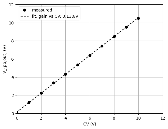
Calibration: apply a test signal (440Hz sine, 8Vpp) to the audio input and a DC 1V level to the CV input. Adjust the trim pot until the output is balanced (mean voltage \simeq 0V).
Measurement: apply a test signal (440Hz sine, 8Vpp) to the audio input and vary the DC level to the CV input.
| CV (V) | Output (Vpp) |
|---|---|
| 1.0 | 1.20 |
| 2.0 | 2.24 |
| 3.0 | 3.36 |
| 4.0 | 4.32 |
| 5.0 | 5.36 |
| 6.0 | 6.40 |
| 7.0 | 7.44 |
| 8.0 | 8.48 |
| 9.0 | 9.52 |
| 10.0 | 10.72 |
The linear fit of the gain response is
A = 0.017 + 0.13V_{cv}
where A is the gain in V/V and V is the CV input in Volts. With R = 56k\Omega in the output stage, the gain at 8V CV input is expected to be 1.04 V/V. The measured gain at 8V CV input is 1.06 (within 2% of expected).
BOM
| Reference | Value | Qty |
|---|---|---|
| C1,C2 | 220p | 2 |
| C3,C4,C5,C7,C8,C9 | 100n | 6 |
| C6,C10 | 10u | 2 |
| D1,D2 | 1N4148 | 2 |
| D3,D4 | 1N5819 | 2 |
| J1,J2,J3,J4,J5,J6 | WQP-PJ323M | 6 |
| J7 | IDC Header 10P | 1 |
| Q1,Q2 | BC557 | 2 |
| R1,R10 | 68k | 2 |
| R2,R11 | 15k | 2 |
| R8,R17 | 56k | 2 |
| R3,R4,R6,R12,R13,R15 | 100k | 6 |
| RV1,RV2 | 3296W 100k | 2 |
| RV3,RV4 | RV09 B100k | 2 |
| R5,R7,R14,R16 | 220R | 4 |
| R9,R18 | 1k | 2 |
| R19,R20 | 10R | 2 |
| U1 | TL074 | 1 |
| U2 | LM13700 | 1 |