State Variable Filter
The last module for 2025! At the beginning of the year, I had a goal to build a new module every two months with the objective of having the core of a synth by the end. With this filter, I think that the basic pieces are in place (although I still have lots of ideas for 2026). The state variable filter is a very elegant textbook design that translates nicely into an analog circuit. The prototype came together well and the filter response fits the theory beautifully. However, there was one issue...
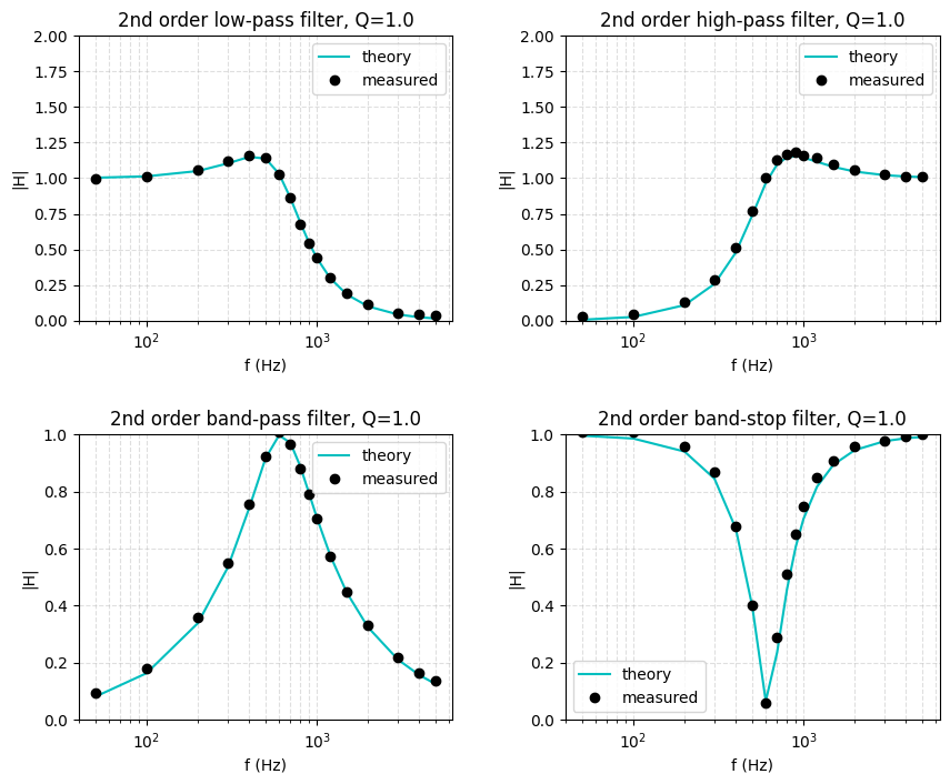
This is another design that works fine on the breadboard, although it requires a breakout for the SOIC packaged LM13700. That enabled me to break the build down into a couple of stages, starting with the linear to exponential voltage conversion. After putting it togeter on the breadboard, I did a very manual filter response measurement: adjust the frequency of the sine source, check the amplitude on the 'scope, goto 0. It was very exciting to see the result:
That left the nagging issue: DC offset. Both the Thomas Henry and Oberheim SEM designs that serve as the reference for this module feature offset trims for the OTAs. At first I didn't pay much attention to this since it wasn't very important in the other design with an OTA (the VCA). When I checked the DC offsets at the filter outputs, I consistently saw \pm 100-300\mathrm{mV} offsets at the HP and BP output, and anything from 0.1 to 1.5V at the LP output!
At first I tried adding the trim pots into the breadboard and twiddling the screws, but it felt like playing whack-a-mole and any adjustment seemed to just send the DC to the rails. When I got the PCBs back, I built it without the trim pots (just the 220s to ground). The same issue was present, so it wasn't just a breadboard quirk. Others that built this filter didn't report these offsets, so I was a bit stuck. I did some testing on the PCB:
- no inputs (audio line in at 0V)
- adjust the resonance and cutoff controls
- cutoff will change the amplifier bias current into the OTAs
- resonance influences the feedback in the filter
- measure the LP, HP & BP outputs
It quickly became clear that there was a pattern:
- the HP & BP outputs had a fairly constant DC offset (in the range from -100mV to -300mV) that didn't depend on either control
- the LP output was sensitive to the resonance control and had the opposite sign to the HP & BP output DC offsets.
- the sign flip is odd because there's no inversion from the second stage (BP) to third stage (LP)
- the DC offset was largest for the lowest resonance setting (as high as 1.5V) and reduced from there
I was committed at this point, so I worked through the derivation, which yields an interesting result. For an offset of \Delta v_1 at the inputs of the first OTA and \Delta v_2 at the inputs of the second OTA, the DC values at the filter outputs are
There are two important ratios that contribute:
- the inverted ratio of the resistor divider used to attenuate the input signal to the OTA, A'_{r} = 100\mathrm{k}/220 (note I use A_r in my derivation as the inverse: A'_{r} \equiv A^{-1}_r).
- the weighting of the resonance feedback signal, A_x = 100\mathrm{k}/R_r, where R_r is the sum of the 22k and the contribution from the resonance pot.
This explains the behavior pretty well:
- the DC offsets see a scaled-up version of the OTA input offsets due to the resistive divider
- typical (datasheet) offsets are 0.3-0.4mV
- A'_r \simeq 500
- the contribution can be \pm 100-300\mathrm{mV}
- only the LP output depends on the resonance feedback weighting and it has the opposite sign to the others
It also suggests a more methodical approach to removing the DC offsets:
- since the HP output only depends on the input offset of the first OTA, zero that first
- since the BP output only depends on the input offset of the second OTA, zero that next
- if both the HP and BP outputs have zero DC offset, \Delta v_1 = \Delta v_2 = 0 and the DC offset should be removed from the LP output
This also explains why I struggled the first time: trying to remove the DC offset by looking at the LP output is complicated by the dependence on the resonance and the contributions from both OTA input offsets.
Since the A'_r factor multiples the OTA input offsets, the result is sensitive to changes on the order of 10's of uVs. Therefore, it's also important to follow the reference designs and
- make sure that the resistive divider for the trim pots is also scaled up by a factor of 10 (and adjustment range of \pm 2\mathrm{mV} is lots)
- start with centered trim pots
In practice, getting everything below 50mV requires a bit of fiddling, but is much improved now and the result is more stable. This worked on both the breadboard prototype and on the first PCB, but I plan to build a couple more and see if I can gather some more statistics. Of course, writing this up now and looking again at the older designs, it very much feels like I'm rediscovering something that was well known 50 years ago, but c'est la vie.